
单击打开
10G SFP+ BIDI 60km
Features
Up to 11.1Gb/s data rate
1270nm DFB laser and APD receiver for HXSX-AL6863x
1330nm DFB laser and APD receiver for HXSX-AL8663x
2-wire interface with integrated Digital Diagnostic monitoring
Up to 60km transmission on SMF
BIDI LC optical connector
Single +3.3V power supply
Metal enclosure, for lower EMI
Maximum power consumption 1.5W
RoHS-6 compliant and lead-free
SFF-8472 MSA compliant &SFF-8431
Operating case temperature
Commercial: 0 ~ 70℃
Applications
Back to Back
10GBASE-ER/EW
10G Ethernet
HXSX-AL6863x/ HXSX-AL8663x SFP+ transceiver is designed for use in 10-Gigabit Ethernet links up to 60km over single mode fiber .The module consists of CWDM DFB Laser, APD and Preamplifier in a high-integrated optical sub-assembly. Digital diagnostics functions are available via a 2-wire serial interface, as specified in SFF-8472.
HXSX-AL6863x/HXSX-AL8663x transceivers provide a unique enhanced digital diagnostic monitoring interface, which allows real-time access to device operating parameters such as transceiver temperature, laser bias current, transmitted optical power, received optical power and transceiver supply voltage. It also defines a sophisticated system of alarm and warning flags, which alerts end-users when particular operating parameters are outside of a factory set normal range.
The SFP+ MSA defines a 256-byte memory map in EEPROM that is accessible over a 2-wire serial interface at the 8 bit address 1010000X (A0h). The digital diagnostic monitoring interface makes use of the 8 bit address 1010001X (A2h), so the originally defined serial ID memory map remains unchanged.
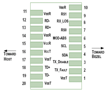
Pin Assignment and Pin Description
|
Pin |
Symbol |
Name/Description |
Notes |
|
VEET |
Transmitter Ground (Common with Receiver Ground) |
1 |
|
|
2 |
TFAULT |
Transmitter Fault. |
2 |
|
3 |
TDIS |
Transmitter Disable. Laser output disabled on high or open. |
3 |
|
4 |
SDA |
2-wire Serial Interface Data Line |
4 |
|
5 |
SCL |
2-wire Serial Interface Clock Line |
4 |
|
6 |
MOD_ABS |
Module Absent. Grounded within the module |
4 |
|
7 |
RS0 |
Rate Select 0 |
5 |
|
8 |
LOS |
Loss of Signal indication. Logic 0 indicates normal operation. |
6 |
|
9 |
RS1 |
No connection required |
|
|
10 |
VEER |
Receiver Ground (Common with Transmitter Ground) |
1 |
|
11 |
VEER |
Receiver Ground (Common with Transmitter Ground) |
1 |
|
12 |
RD- |
Receiver Inverted DATA out. AC Coupled |
|
|
13 |
RD+ |
Receiver Non-inverted DATA out. AC Coupled |
|
|
14 |
VEER |
Receiver Ground (Common with Transmitter Ground) |
1 |
|
15 |
VCCR |
Receiver Power Supply |
|
|
16 |
VCCT |
Transmitter Power Supply |
|
|
17 |
VEET |
Transmitter Ground (Common with Receiver Ground) |
1 |
|
18 |
TD+ |
Transmitter Non-Inverted DATA in. AC Coupled. |
|
|
19 |
TD- |
Transmitter Inverted DATA in. AC Coupled. |
|
|
20 |
VEET |
Transmitter Ground (Common with Receiver Ground) |
1 |
Notes:
1. Circuit ground is internally isolated from chassis ground.
2. TFAULT is an open collector/drain output, which should be pulled up with a 4.7kΩ– 10 kΩ resistor on the host board if intended for use. Pull up voltage should be between 2.0V to Vcc + 0.3V.A high output indicates a transmitter fault caused by either the TX bias current or the TX output power exceeding the preset alarm thresholds. A low output indicates normal operation. In the low state, the output is pulled to <0.8V.
3. Laser output disabled on TDIS >2.0V or open, enabled on TDIS <0.8V.
4. Should be pulled up with 4.7kΩ- 10kΩ on host board to a voltage between 2.0V and 3.6V. MOD_ABS pulls line low to indicate module is plugged in.
5. Internally pulled down per SFF-8431 Rev 4.1.
6. LOS is open collector output. It should be pulled up with 4.7kΩ – 10kΩ on host board to a voltage between 2.0V and 3.6V. Logic 0 indicates normal operation; logic 1 indicates loss of signal.
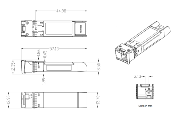
Mechanical Dimensions
Absolute Maximum Ratings
It has to be noted that the operation in excess of any individual absolute maximum ratings might cause permanent damage to this module.
|
Parameter |
Symbol |
Min |
Max |
Unit |
Notes |
|
Storage Temperature |
TS |
-40 |
85 |
oC |
|
|
Power Supply Voltage |
VCC |
-0.5 |
3.6 |
V |
|
|
Relative Humidity (non-condensation) |
RH |
5 |
95 |
% |
|
|
Damage Threshold |
THd |
0 |
|
dBm |
|
Recommended Operating Conditions and Power Supply Requirements
|
Parameter |
Symbol |
Min |
Typical |
Max |
Unit |
Notes |
|
TOP |
0 |
|
70 |
oC |
commercial |
|
|
Power Supply Voltage |
VCC |
3.135 |
3.3 |
3.465 |
V |
|
|
Data Rate |
|
|
10.3125 |
|
Gb/s |
|
|
Control Input Voltage High |
|
2 |
|
Vcc |
V |
|
|
Control Input Voltage Low |
|
0 |
|
0.8 |
V |
|
|
Link Distance (SMF) |
D |
|
|
60 |
km |
9/125um |
Electrical Characteristics
The following electrical characteristics are defined over the Recommended Operating Environment unless otherwise specified.
|
Parameter |
Symbol |
Min. |
Typ. |
Max |
Unit |
Notes |
|
Power Consumption |
p |
|
|
1.5 |
W |
|
|
Supply Current |
Icc |
|
|
450 |
mA |
|
|
|
||||||
|
Single-ended Input Voltage Tolerance |
Vcc |
-0.3 |
|
4.0 |
V |
|
|
AC Common Mode Input Voltage Tolerance (RMS) |
|
15 |
|
|
mV |
|
|
Differential Input Voltage Swing |
Vin,pp |
180 |
|
700 |
mVpp |
|
|
Differential Input Impedance |
Zin |
90 |
100 |
110 |
Ohm |
1 |
|
Transmit Disable Assert Time |
|
|
|
10 |
us |
|
|
Transmit Disable Voltage |
Vdis |
Vcc-1.3 |
|
Vcc |
V |
|
|
Transmit Enable Voltage |
Ven |
Vee |
|
Vee +0.8 |
V |
2 |
|
Receiver |
||||||
|
Differential Output Voltage Swing |
Vout,pp |
300 |
|
850 |
mVpp |
|
|
Differential Output Impedance |
Zout |
90 |
100 |
110 |
Ohm |
3 |
|
Data output rise/fall time |
Tr/Tf |
28 |
|
|
ps |
4 |
|
LOS Assert Voltage |
VlosH |
Vcc-1.3 |
|
Vcc |
V |
5 |
|
LOS De-assert Voltage |
VlosL |
Vee |
|
Vee +0.8 |
V |
5 |
|
Power Supply Rejection |
PSR |
100 |
|
|
mVpp |
6 |
Notes:
1. Connected directly to TX data input pins. AC coupled thereafter.
2. Or open circuit.
3. Input 100 ohms differential termination.
4. These are unfiltered 20-80% values.
5. Loss of Signal is LVTTL. Logic 0 indicates normal operation; logic 1 indicates no signal detected.
6. Receiver sensitivity is compliant with power supply sinusoidal modulation of 20 Hz to 1.5 MHz up to specified value applied through the recommended power supply filtering network.
Optical Characteristics
|
Parameter |
Symbol |
Min. |
Typical |
Max |
Unit |
Notes |
|
Transmitter |
||||||
|
Center Wavelength |
λC |
1260 |
1270 |
1280 |
nm |
|
|
1320 |
1330 |
1340 |
nm |
|||
|
Optical Spectral Width |
∆λ |
|
|
1 |
nm |
|
|
Side Mode Suppression Ratio |
SMSR |
30 |
|
|
dB |
|
|
Average Optical Power |
PAVG |
0 |
|
5 |
dBm |
|
|
Optical Extinction Ratio |
ER |
3.5 |
|
|
dB |
|
|
Average Launched Power(Laser Off) |
Poff |
|
|
-30 |
dBm |
|
|
Transmitter Eye Mask |
Compliant with IEEE802.3ae |
|
||||
|
Receiver |
||||||
|
Center Wavelength |
λC |
1320 |
1330 |
1340 |
nm |
HXSX-AL8663x |
|
1260 |
1270 |
1280 |
nm |
HXSX-AL6863x |
||
|
Receiver Sensitivity (Average Power) |
Sen. |
|
|
-20 |
dBm |
1 |
|
Input Saturation Power (overload) |
Psat |
-6 |
|
|
dBm |
|
|
LOS Assert |
LOSA |
-35 |
|
|
dBm |
|
|
LOS De-assert |
LOSD |
|
|
-21 |
dBm |
|
|
LOS Hysteresis |
LOSH |
0.5 |
|
|
dB |
|
The following optical characteristics are defined over the Recommended Operating Environment unless otherwise specified.
Notes:
1. Measured with Light source 1270nm@1330nm, ER=3.5dB; BER =<10^-12 @10.3125Gbps, PRBS=2^31-1 NRZ.
Digital Diagnostic Functions
The following digital diagnostic characteristics are defined over the Recommended Operating Environment unless otherwise specified. It is compliant to SFF8472 Rev10.2 with internal calibration mode. For external calibration mode please contact our sales staff.
|
Parameter |
Symbol |
Min. |
Max |
Unit |
Notes |
|
Temperature monitor absolute error |
DMI_ Temp |
-3 |
3 |
degC |
Over operating temp |
|
Supply voltage monitor absolute error |
DMI _VCC |
-0.15 |
0.15 |
V |
Full operating range |
|
RX power monitor absolute error |
DMI_RX |
-3 |
3 |
dB |
|
|
Bias current monitor |
DMI_ bias |
-10% |
10% |
mA |
|
|
TX power monitor absolute error |
DMI_TX |
-3 |
3 |
dB |
|
