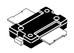
A 31W N-Channel LDMOS RF power transistor designed for broadcasttransmitter applications with frequencies from 136 to 941MHz. The high gain, ruggedness and Broadband performance of this device make it ideal for large–signal, common–source amplifier applications in digital transmitter applications.
Ÿ Production test performance ( TA=25°C , CW class-AB)
F (MHz) | VDS(V) | IDQ(mA) | PL(W) | Gp(dB) | ηD (%) |
860 | 28 | 100 | 31 | 15 | 65 |
Ÿ Load Mismatch /Ruggedness
F (MHz) | VSWR | Pin(W) | Test Voltage | Result |
860 | >10:1 at all Phase Angles | 1.0 (3dB Overdrive) | 32Vdc | No Device Degradation |
Ÿ Integrated ESD protection
Ÿ
Unmatched Input and Output Allowing Wide Frequency Range Utilization
Ÿ Integrated Stability Enhancements
Ÿ Excellent ruggedness
Ÿ High power gain
Ÿ High efficiency
Ÿ Excellent reliability
Ÿ Easy power control
Ÿ Suitable for linear application: TETRA,SSB,LTE
Ÿ In Tape and Reel. T1 Suffix = 500 Units, 24 mm Tape Width, 13 inch Reel.
Ÿ Output Stage VHF/UHF Band Mobile Radio
Ÿ Industrial, scientific and medical applications
Ÿ Driver for 10–1000 MHz Applications
2. Maximum ratings
Table 1. Maximum ratings
Rating | Symbol | Value | Unit |
Drain–Source Voltage | VDSS | -0.5, +65 | Vdc |
Gate–Source Voltage | VGS | -5, +6 | Vdc |
Storage Temperature Range | Tstg | –65 to +150 | °C |
Case Operating Temperature | TC | 150 | °C |
Operating Junction Temperature | TJ | 150 | °C |
3. Thermal characteristics
Table 2. Thermal characteristics
Symbol | Parameter | Conditions | Typ | Unit |
Rth(j-c) | thermal resistance from junction to case | Tcase = 79℃; PL =31W (CW) | 0.63 | ℃/W |
4. ESD Protection Characteristics
Table 3. Thermal characteristics
Test Methodology | Class |
Human Body Model | 2B |
Tj = 25℃ unless otherwise specified
Characteristic | Symbol | Min | Typ | Max | Unit |
Drain–Source Breakdown Voltage (VGS = 0, ID = 10µAdc) | V(BR)DSS | 70 | — | — | Vdc |
Zero Gate Voltage Drain Current (VDS =28 Vdc, VGS = 0) | IDSS | — | — | 1 | µAdc |
Gate–Source Leakage Current (VGS =5 Vdc, VDS = 0) | IGSS | — | — | 1 | µAdc |
Gate Threshold Voltage (VDS = 10 Vdc, ID = 1mAdc) | VGS(th) | 0.5 | 1.0 | 1.5 | Vdc |
Gate Quiescent Voltage (VDS =28 Vdc, ID = 100mAdc) | VGS(q) | 1.0 | 1.5 | 3.0 | Vdc |
Drain cut-off current (VDS =10 Vdc, VGS = 6Vdc) | IDSX | 17 | 22 | — | Adc |
Drain–Source on-state resistance (VGS = 6 Vdc, ID = 3.7 A) | RDS(on) | — | 0.24 | — | Ω |
Input Capacitance (VDS = 32 Vdc, VGS = 0, f = 1.0 MHz) | Ciss | — | 170 | — | pF |
Output Capacitance (VDS = 32 Vdc, VGS = 0, f = 1.0 MHz) | Coss | — | 60 | — | pF |
Reverse Transfer Capacitance (VDS = 32 Vdc, VGS = 0, f = 1.0 MHz) | Crss | — | 10 | — | pF |
Table 5. RF functional characteristics
Mode of operation: CW; f = 860 MHz; RF performance at VDS = 28 V; IDq = 100 mA; Tcase = 25℃;
Symbol | Characteristic | Condition | Min | Typ | Max | Unit |
GP | Power Gain | PL = 31 W VDS = 28 V IDQ=100mA f = 860 MHz | 15 | 16 | — | dB |
ηD | Drain Efficiency | 60 | 65 | — | % |
6. Test information
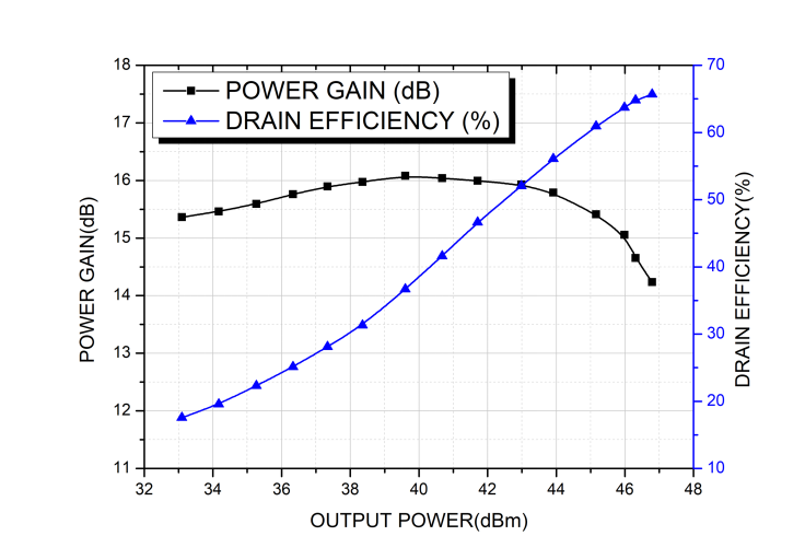
VDD=28V,f=860MHz,IDQ=100mA
Fig 1.Power gain and drain efficiency as function of load power; typical values
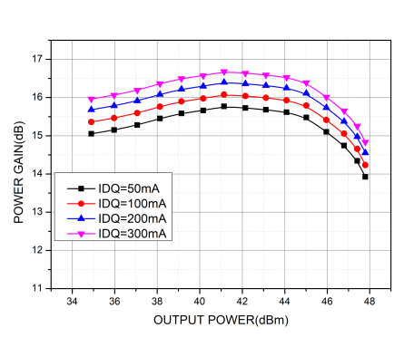
f=860MHz, VDD=28V
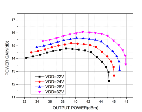
f=860MHz IDQ=100mA
Fig 2. Power Gain versus Output Power
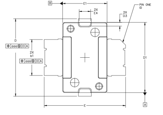
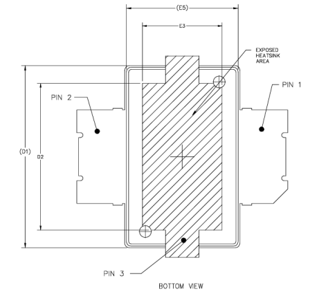
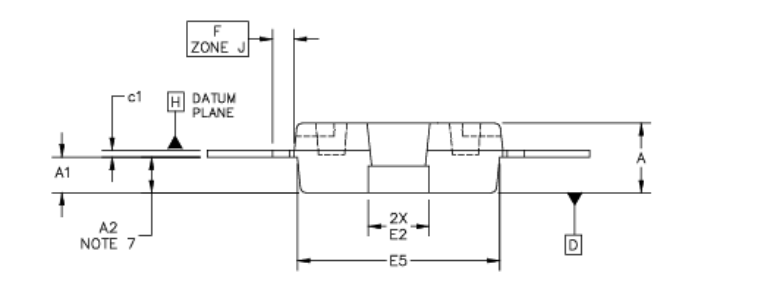
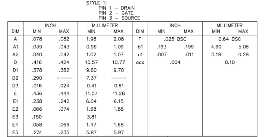
TO270-2
