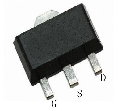
 N-Channel Enhancement-Mode MOSFET
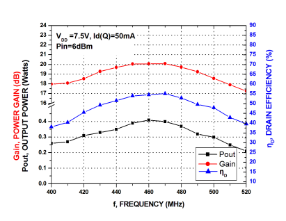
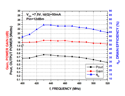
Typical Broadband EVB Performance (IDQ=50mA, TA = 25℃, CW)
VDD | Freq. | Gmax | Pout | PAE | |
[V] | [MHz] | [dB] | [dBm] | [Watts] | [%] |
7.5 | 400 | 19.8 | 28.3 | 0.67 | 59.6 |
440 | 20.7 | 29.2 | 0.83 | 76.9 | |
480 | 21.0 | 28.9 | 0.77 | 74.6 | |
520 | 17.9 | 28.6 | 0.73 | 71.1 | |
Ÿ Capable of handling 20:1 VSWR @ 9Vdc, 0.8Watts, CW
Features
Ÿ Characterized for Operation from 136 to 941 MHz
Ÿ Unmatched Input and Output Allowing Broad Frequency Range Utilization
Ÿ Integrated ESD Protection
Ÿ Broadband – Full Power Across the Band
Ÿ Exceptional Thermal Performance
Ÿ Extreme Ruggedness
Typical Applications
Ÿ Output Stage VHF Band Handheld Radio
Ÿ Output Stage UHF Band Handheld Radio
Ÿ Output Stage for 700–800 MHz Handheld Radio
Ÿ Driver for 10–1000 MHz Applications
Table1. Maximum Ratings
Rating | Symbol | Value | Unit |
Drain-Source Voltage | VDSS | –0.5, +20 | Vdc |
Gate-Source Voltage | VGS | –0.5, +8 | Vdc |
Operating Voltage | VDD | +0, +9 | Vdc |
Storage Temperature Range | Tstg | –65 to +150 | ℃ |
Case Operating Temperature | TC | –40 to +150 | ℃ |
Operating Junction Temperature | TJ | –40 to +150 | ℃ |
Power Dissipation @TC=25℃ | PD | 3.0 | Watts |
Table 2. ESD Protection Characteristics
Test Methodology | Class |
Human Body Model (per JESD22--A114) | 2, passes 2500 V |
Machine Model (per EIA/JESD22--A115) | A, passes 100 V |
Charge Device Model (per JESD22--C101) | IV, passes 2000 V |
Table 3. Electrical Characteristics (TA=25℃ unless otherwise noted)
Characteristic | Symbol | Min | Typ. | Max | Unit |
Off Characteristics
Gate-Source Leakage Current (VGS=5Vdc, VDS=0Vdc) | IGSS | - | - | 500 | nAdc |
Zero Gate Voltage Drain Leakage Current (VDS=16Vdc, VGS=0Vdc) | IDSS | - | - | 1 | uAdc |
Zero Gate Voltage Drain Leakage Current (VDS=7.5Vdc, VGS=0Vdc) | IDSS | - | - | 500 | nAdc |
On Characteristics
Gate Threshold Voltage (VDS=7.5Vdc, ID=1mA) | VGS(th) | 1.6 | 1.8 | 2.0 | Vdc |
Gate Quiescent Voltage (VDD=7.5Vdc, ID=50mA Measured in Functional Test) | VGS(Q) | 2.2 | 2.4 | 2.8 | Vdc |
Drain-Source On-Voltage (VGS=5Vdc, ID=100mA) | VDS(ON) | - | 0.25 | - | Vdc |
Dynamic Characteristics
Reverse Transfer Capacitance (VDG=7.5V, Level=30mVac@1MHz) | Crss | - | 0.21 | - | pF |
Output Capacitance (VDS=7.5V, Level=30mVac@1MHz) | Coss | - | 1.6 | - | pF |
Input Capacitance (VGS=5V, Level=30mVac@1MHz) | Ciss | - | 8.0 | - | pF |
Typical Performances (In DuSemi Narrowband Test DEMO, 50 Ohm system)
Frequency=440MHz, VDD=7.5Vdc, ID(Q)=50mA, Pin=9dBm, TA=25℃
Output Power | Pout | - | 0.61 | - | Watts |
Power Gain | GPS | - | 19.0 | - | dB |
Drain Efficiency
| ηD | - | 66.5 | - | % |
Broad Band Evaluation Circuit (@VDD = 7.5V, f = 440 MHz)
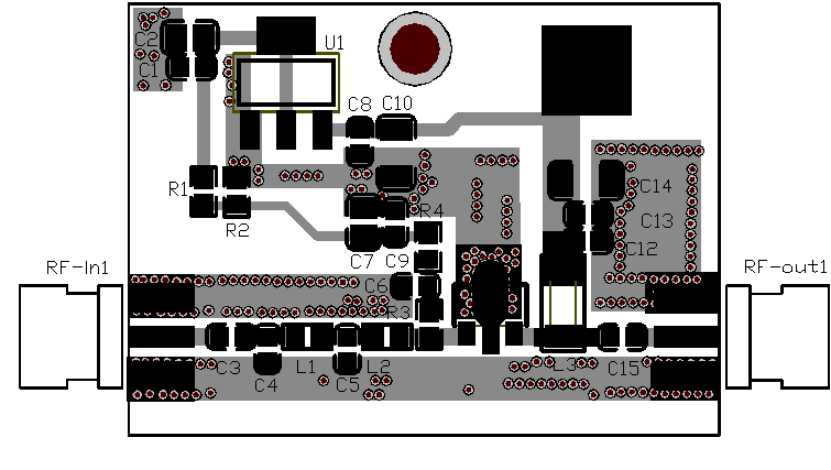
Test Circuit Component Layout
Table 4. Test Circuit Component Designations and Value
Part | Description | Part Number | Manufacturer |
R3 | 470Ohm | — | — |
R4 | 6.8KOhm | — | — |
L1, L2 | 4.7nH | — | — |
L3 | 8 Turns D: 0.5 mm, φ 2.4 mm Enamel Wire | — | — |
C3,C15, | 100pF Chip Capacitors | GQM21P5C1H101JB01 | Murata |
C4 | 18pF Chip Capacitors | GRM1885C1H201JA01 | Murata |
C12, C9 | 1000pF Chip Capacitors | GRM1885C1H102JA01 | Murata |
C10, C14,C7 | 10uF,25VChip Capacitors | — | — |
C5 | 24pF Chip Capacitors | — | Murata |
R1,R2,C1,C2,C8,C6 | NC | — | — |
U1 | LM1117 | ||
PCB | FR-4 ,1.6mm, Ɛr4.5 | — | — |
Typical Characterisitics
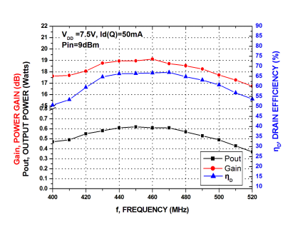
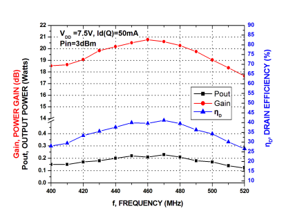
1、Power Gain, Drain Efficiency and Output Power versus Frequency at a Constant Pin
VDD | ID(Q) | Pin | Freq | Pout | Gain | ηD | |
[V] | [mA] | [dBm] | [MHz] | [dBm] | [Watts] | [dB] | [%] |
7.5 | 50 | 9 | 400 | 26.7 | 0.47 | 17.6 | 50.7 |
440 | 27.9 | 0.61 | 19.0 | 66.5 | |||
480 | 27.6 | 0.57 | 18.5 | 64.8 | |||
520 | 25.7 | 0.37 | 16.8 | 53.7 | |||
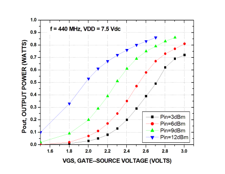
2. Output Power versus Gate-Source Voltage @440MHz
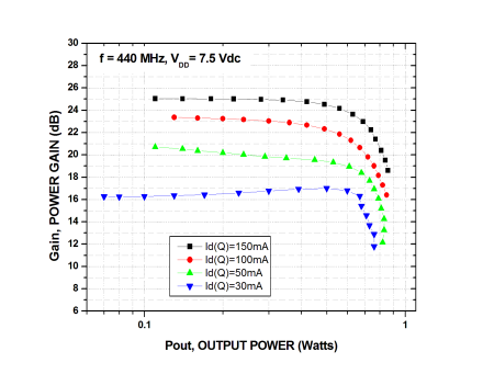
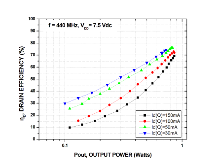
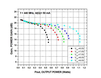
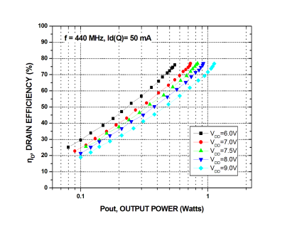
3. Power Gain and Drain Efficiency versus Output Power@440MHz
Freq | VDD | ID(Q) | Pout | Gain | PAE | |
[MHz] | [V] | [mA] | [dBm] | [Watts] | [dB] | [%] |
440 | 7.5 | 30 | 28.8 | 0.76 | 17.0 | 74.4 |
50 | 29.2 | 0.83 | 20.7 | 76.9 | ||
100 | 29.4 | 0.87 | 23.8 | 73.4 | ||
150 | 29.5 | 0.89 | 25.6 | 69.3 | ||
Freq | ID(Q) | VDD | Pout | Gain | PAE | |
[MHz] | [mA] | [V] | [dBm] | [Watts] | [dB] | [%] |
440 | 50 | 6.0 | 27.4 | 0.55 | 21.0 | 76.6 |
7.0 | 28.6 | 0.73 | 20.8 | 76.7 | ||
7.5 | 29.2 | 0.83 | 20.7 | 76.9 | ||
8.0 | 29.6 | 0.92 | 20.8 | 76.8 | ||
9.0 | 30.5 | 1.12 | 20.8 | 76.7 | ||
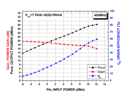
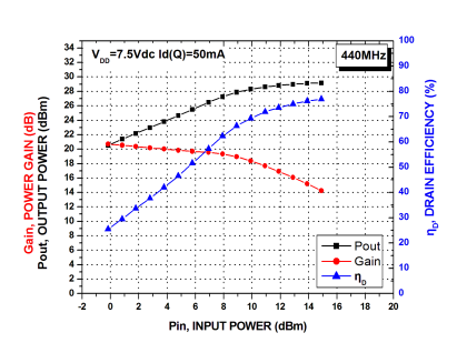
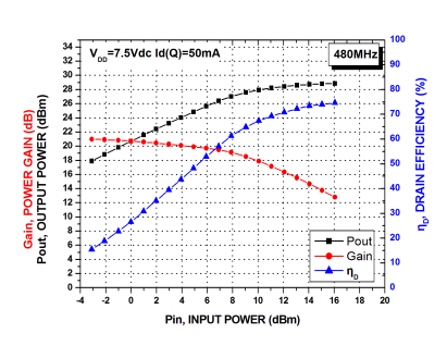
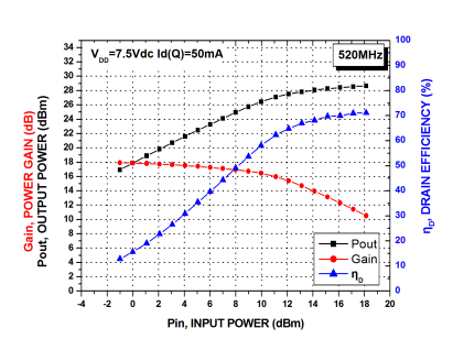
4. Power Gain, Drain Efficiency and Output Power versus Input Power
VDS | ID(Q) | Freq. | Gain | Pout | ηD | |
[V] | [mA] | [MHz] | [dB] | [dBm] | [Watts] | [%] |
7.5 | 50 | 400 | 19.8 | 28.3 | 0.67 | 59.6 |
440 | 20.7 | 29.2 | 0.83 | 76.9 | ||
480 | 21.0 | 28.9 | 0.77 | 74.6 | ||
520 | 17.9 | 28.6 | 0.73 | 71.1 | ||
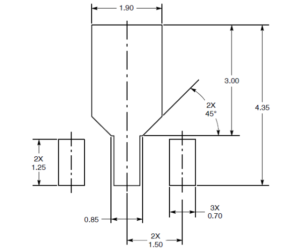
PCB Pad Layout for SOT– 89
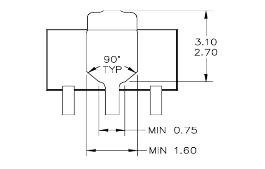
Bottom View
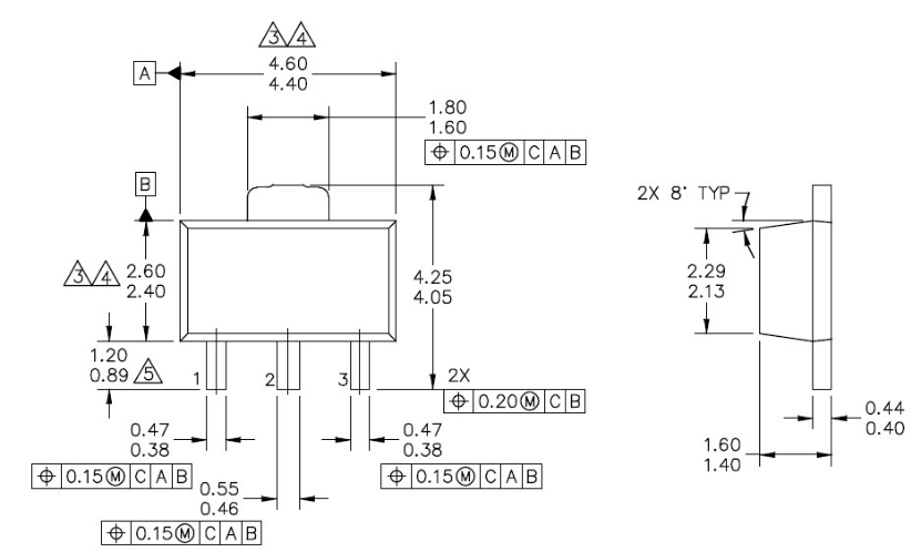
PACKAGE DIMENSIONS
Если вам нужна дополнительная информация, пожалуйста, свяжитесь с нами.