
单击打开
10G GPON ONU
PRODUCT FEATURES
1270nm DFB Burst mode transmitter, APD Continuous Mode Receiver
Compliant with ITU-G.987.2
SFP+ MSA SFF-8431 compliant
Digital diagnostic SFF-8472 compliant
SFP+ package with SC receptacle
Single + 3.3V Power Supply
ROHS-6/6 compliant
Laser Class 1 Product which comply with the Requirements of IEC 60825-1 and IEC 60825-2
APPLICATIONS
XGPON ONU
Burst Mode application
FTTX WDM Broadband Access
PRODUCT DESCRIPTION
HC’s 10G GPON ONU transceiver GX-U1221-20D is designed for Gigabit Ethernet Passive Optical Network transmission. The module is contained in a SFP+ package with SC/UPC receptacle connector. It consists 1270nm DFB laser, APD+TIA, Preamplifier and WDM filter in a high-integrated optical sub-assembly, and it receives up to 9.953Gbps of continuous mode data at 1577nm, and transmits 2.488Gbps of burst mode data at 1270 nm .
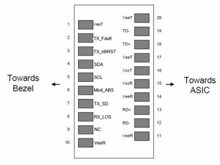
Pin Description
|
Pin |
Symbol |
Name/Description |
Ref. |
|
1 |
VeeT |
Transmitter Ground |
1 |
|
2 |
TX_Fault |
Transmitter Fault. |
|
|
3 |
TX_nBRST |
Transmitter Burst Control |
|
|
4 |
SDA |
2 wire Serial Interface Data Line(MOD_DEF2) |
2 |
|
5 |
SCL |
2 wire Serial Interface Clock(MOD_DEF1) |
|
|
6 |
Mod_ABS |
Module Absent, Connect to VeeT or VeeR in the module(MOD_DEF0) |
|
|
7 |
TX_SD |
TX signal Detect |
3 |
|
8 |
RX_LOS |
Loss of Signal indication. |
4 |
|
9 |
NC |
Not Connected |
|
|
10 |
VeeR |
Receiver Ground |
1 |
|
11 |
VeeR |
Receiver Ground |
1 |
|
12 |
RD- |
Receiver Inverted DATA out. AC Coupled |
|
|
13 |
RD+ |
Receiver Non-inverted DATA out. AC Coupled |
|
|
14 |
VeeR |
Receiver Ground |
1 |
|
15 |
VccR |
Receiver Power Supply |
|
|
16 |
VccT |
Transmitter Power Supply |
|
|
17 |
VeeT |
Transmitter Ground |
1 |
|
18 |
TD+ |
Transmitter Non-Inverted DATA in. AC Coupled. |
|
|
19 |
TD- |
Transmitter Inverted DATA in. AC Coupled. |
|
|
20 |
VeeT |
Transmitter Ground |
1 |
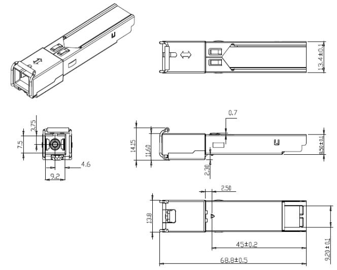
Outline Dimensions
Absolute Maximum Ratings
|
Parameter |
Symbol |
Min. |
Typ. |
Max. |
Unit |
Note |
|
Storage Temperature |
Ts |
-40 |
|
85 |
ºC |
|
|
Storage Ambient Humidity |
HA |
5 |
|
95 |
% |
|
|
Power Supply Voltage |
VCC |
-0.3 |
|
3.7 |
V |
|
|
Signal Input Voltage |
|
-0.3 |
|
Vcc+0.3 |
V |
|
|
Receiver Damage Threshold |
|
5 |
|
|
dBm |
|
Recommended Operating Conditions
|
Parameter |
Symbol |
Min. |
Typ. |
Max. |
Unit |
Note |
|
Case Operating Temperature |
Tcase |
0 |
|
70 |
ºC |
Without air flow |
|
Ambient Humidity |
HA |
5 |
|
70 |
% |
Non-condensing |
|
Power Supply Voltage |
VCC |
3.13 |
3.3 |
3.47 |
V |
|
|
Power Supply Current |
ICC |
|
|
450 |
mA |
|
|
Power Supply Noise Rejection |
|
|
|
100 |
mVp-p |
100Hz to 1MHz |
|
Data Rate |
DR |
|
2488 |
|
Mbps |
|
|
Coupled fiber |
Single mode fiber |
9/125um |
||||
Specification of Transmitter
|
Parameter |
Symbol |
Min. |
Typ. |
Max. |
Unit |
Note |
|
Average Launched Power |
PO |
2 |
|
7 |
dBm |
|
|
Extinction Ratio |
ER |
8.2 |
|
|
dB |
|
|
Center Wavelength |
λC |
1260 |
|
1280 |
nm |
DFB Laser |
|
Side mode suppression ratio |
SMSR |
30 |
|
|
dB |
|
|
Spectrum Bandwidth(-20dB) |
σ |
|
|
1 |
nm |
|
|
Optical Rise/Fall Time |
tr/tf |
|
|
140 |
ps |
Note (1) |
|
Transmitter OFF Output Power |
POff |
|
|
-45 |
dBm |
|
|
Total Jitter |
|
|
|
0.2 |
UI |
|
|
Output Eye Mask |
Compliant with ITU G.987.2 |
|
|
|||
Note (1). These are unfiltered 20-80% values, Measure at 2^7-1 NRZ PRBS pattern (2.488Gbps)
Specification of Receiver
|
Parameter |
Symbol |
Min. |
Typ. |
Max. |
Unit |
Note |
|
Input Optical Wavelength |
λIN |
1575 |
|
1580 |
nm |
APD |
|
Receiver Sensitivity |
Psen1 |
|
|
-28 |
dBm |
Note (1) |
|
|
Psen2 |
|
|
-24 |
dBm |
|
|
Input Saturation Power (Overload) |
PSAT |
-8 |
|
|
dBm |
|
|
Los Of Signal Assert |
PA |
|
|
-29 |
dBm |
|
|
Los Of Signal De-assert |
PD |
-40 |
|
|
dBm |
Note (2) |
|
LOS Hysteresis |
PA-PD |
0.5 |
2 |
6 |
dB |
|
|
Tolerance to reflected optical power |
|
|
|
12 |
dB |
|
Note (1):Measured with Light source ER=8.2dB; BER =<10-3 @PRBS=2^23-1 NRZ
Measured with Light source ER=8.2dB; BER =<10-10 @PRBS=2^23-1 NRZ
Note (2):When SD de-asserted, the data output is Low-level (fixed)
Electrical Interface Characteristics
|
Parameter |
Symbol |
Min. |
Typ. |
Max. |
Unit |
Note |
|
Transmitter |
||||||
|
Differential line input Impedance |
RIN |
90 |
100 |
110 |
Ohm |
|
|
Differential Data Input Swing |
VDT |
200 |
|
1600 |
mVp-p |
Note (1) |
|
BiasCNT(n) Input Voltage- High |
VBCH |
2 |
|
Vcc+0.3 |
V |
LVTTL |
|
BiasCNT(n) Input Voltage- Low |
VBCL |
0 |
|
0.8 |
V |
|
|
Receiver |
||||||
|
Differential Data Output Swing |
VDR |
500 |
|
1000 |
mVp-p |
Note (1) |
|
Signal Detect Output Voltage-High |
VLOSH |
2 |
|
Vcc+0.3 |
V |
LVTTL |
|
Signal Detect Output Voltage-Low |
VLOSL |
0 |
|
0.8 |
V |
|
