
单击打开
10G EPON ONU 30km
PRODUCT FEATURES
IEEE802.3av Gigabit Ethernet compliant
SFP+ package with SC Receptacle
1270nm DFB Burst Mode 10.3125Gbps transmitter, APD TIA Continuous Mode 10.3125Gbps Receiver
Single +3.3V power supply
SFP+ MSA SFF-8431 compliant
Digital Diagnostic SFF-8472 compliant
Case operation temperature:0~70 ℃
LVTTL Bias Control input and Rx Signal Detect output
Laser Class 1 Product which comply with the Requirements of IEC 60825-1 and IEC 60825-2
APPLICATIONS
IEEE 802.3av 10GBASE-PR30
Burst Mode Application
FTTx WDM Broadband Access
PRODUCT DESCRIPTION
HC’s 10G EPON ONU transceiver EX-U1211-30D is designed for Gigabit Ethernet Passive Optical Network transmission. The module is contained in a SFP+ package with SC/UPC receptacle connector. The module consists 1270nm DFB laser, APD+TIA, Preamplifier and WDM filter in a high-integrated optical sub-assembly, and it receives up to 10.3125Gbps of continuous data at 1577nm, and transmits 10.3125Gbps of burst-mode data at 1270nm.
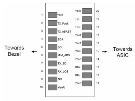
Pin Description
|
Pin |
Symbol |
Name/Description |
Ref. |
|
1 |
VeeT |
Transmitter Ground |
1 |
|
2 |
TX_Fault |
Transmitter Fault. |
|
|
3 |
TX_nBRST |
Transmitter Burst Control |
|
|
4 |
SDA |
2 wire Serial Interface Data Line(MOD_DEF2) |
2 |
|
5 |
SCL |
2 wire Serial Interface Clock(MOD_DEF1) |
|
|
6 |
Mod_ABS |
Module Absent, Connect to VeeT or VeeR in the module(MOD_DEF0) |
|
|
7 |
TX_SD |
TX signal Detect |
3 |
|
8 |
RX_LOS |
Loss of Signal indication. |
4 |
|
9 |
NC |
Not Connected |
|
|
10 |
VeeR |
Receiver Ground |
1 |
|
11 |
VeeR |
Receiver Ground |
1 |
|
12 |
RD- |
Receiver Inverted DATA out. AC Coupled |
|
|
13 |
RD+ |
Receiver Non-inverted DATA out. AC Coupled |
|
|
14 |
VeeR |
Receiver Ground |
1 |
|
15 |
VccR |
Receiver Power Supply |
|
|
16 |
VccT |
Transmitter Power Supply |
|
|
17 |
VeeT |
Transmitter Ground |
1 |
|
18 |
TD+ |
Transmitter Non-Inverted DATA in. AC Coupled. |
|
|
19 |
TD- |
Transmitter Inverted DATA in. AC Coupled. |
|
|
20 |
VeeT |
Transmitter Ground |
1 |
Notes:
1. Circuit ground is internally isolated from chassis ground.
2. SDA is open collector output. Should be pulled up with 4.7k - 10kohms to VccT in the module.
3. TX signal Detect, TX Active State:High.
LOS is open collector output. Should be pulled up with 4.7k - 10kohms on host board to a voltage between 2.0V and 3.6V. Logic 0 indicates normal operation; logic 1 indicates loss of signal.
Outline Dimensions

Absolute Maximum Ratings
|
Parameter |
Symbol |
Min. |
Typ. |
Max. |
Unit |
Note |
|
Storage Temperature |
Ts |
-40 |
|
85 |
ºC |
|
|
Storage Ambient Humidity |
HA |
5 |
|
95 |
% |
|
|
Power Supply Voltage |
VCC |
-0.3 |
|
4 |
V |
|
|
Signal Input Voltage |
|
-0.3 |
|
Vcc+0.3 |
V |
|
|
Receiver Damage Threshold |
|
5 |
|
|
dBm |
|
Recommended Operating Conditions
|
Parameter |
Symbol |
Min. |
Typ. |
Max. |
Unit |
Note |
|
Case Operating Temperature |
Tcase |
0 |
|
70 |
ºC |
|
|
Ambient Humidity |
HA |
5 |
|
95 |
% |
Non-condensing |
|
Power Supply Voltage |
VCC |
3.13 |
3.3 |
3.47 |
V |
|
|
Power Supply Current |
ICC |
|
|
660 |
mA |
|
|
Power Supply Noise Rejection |
|
|
|
100 |
mVp-p |
100Hz to 1MHz |
|
Data Rate |
DR |
10.3125-100ppm |
10.3125 |
10.3125+100ppm |
Gbps |
|
|
Coupled fiber |
Single mode fiber |
9/125um SMF |
||||
Specification of Transmitter
|
Parameter |
Symbol |
Min. |
Typ. |
Max. |
Unit |
Note |
|
Average Launched Power |
PO |
4 |
|
9 |
dBm |
Note (1) |
|
Extinction Ratio |
ER |
6 |
|
|
dB |
|
|
Center Wavelength |
λC |
1260 |
|
1280 |
nm |
DFB Laser |
|
Spectrum Width (-20dB) |
σ |
|
|
1 |
nm |
|
|
Side Mode Suppression Ratio |
SMSR |
30 |
|
|
nm |
|
|
Transmitter OFF Output Power |
POff |
|
|
-45 |
dBm |
|
|
Total Jitter |
tJ |
|
|
0.35 |
UI |
Note (2) |
|
Optical Return Loss Tolerance |
ORLT |
|
|
15 |
dB |
|
|
Relative Intensity Noise |
RIN15OMA |
|
|
-128 |
dB/Hz |
|
|
Optical Transmitter Reflectance |
|
|
|
-10 |
dB |
|
|
Output Eye Mask |
Compliant with IEEE 802.3av |
|
Note (3) |
|||
Note (1). Launched power (avg.) is power coupled into
a single mode fiber with master connector.(Before of Life) Note (2). Measure at 2^31-1 NRZ PRBS pattern
Note (3). Transmitter eye mask definition
Specification of Receiver
|
Parameter |
Symbol |
Min. |
Typ. |
Max. |
Unit |
Note |
|
|
Input Optical Wavelength |
λIN |
1575 |
1577 |
1580 |
nm |
|
|
|
Receiver Sensitivity |
Psen1 |
|
|
-24.5 |
dBm |
Note (1) |
|
|
Psen2 |
|
|
-28.5 |
dBm |
|||
|
Input Saturation Power (Overload) |
PSAT |
-8 |
|
|
dBm |
|
|
|
Los Of Signal Assert |
PA |
|
|
-30 |
dBm |
|
|
|
Los Of Signal De-assert |
PD |
-38 |
|
|
dBm |
Note (2) |
|
|
LOS Hysteresis |
PA-PD |
0.5 |
2 |
6 |
dB |
|
|
|
Receiver Reflectance |
1580 to 1600nm |
|
|
|
-12 |
dB |
Note (3) |
|
Optical Isolation from External Source |
1260 to 1360nm |
|
|
|
-43 |
dB |
|
Note (1). Psen1 measured with Light source 1577nm, ER=9dB; BER =<10-10@PRBS=2^31 NRZ Psen2 measured with Light source 1577nm, ER=9dB; BER =<10-3@PRBS=2^31 NRZ
Note (2). When LOS de-asserted, the RX data+/- output is High-level (fixed) Note (3). Measured at wavelength of 1577nm.
Electrical Interface Characteristics
|
Parameter |
Symbol |
Min. |
Typ. |
Max. |
Unit |
Note |
|
Transmitter |
||||||
|
Differential line input Impedance |
RIN |
90 |
100 |
110 |
Ohm |
|
|
Differential Data Input Swing |
VDT |
200 |
|
1600 |
mVp-p |
Note (1) |
|
BiasCNT(n) Input Voltage- High |
VBCH |
2 |
|
Vcc+0.3 |
V |
LVTTL |
|
BiasCNT(n) Input Voltage- Low |
VBCL |
0 |
|
0.8 |
V |
|
|
Receiver |
||||||
|
Differential Data Output Swing |
VDR |
500 |
|
1000 |
mVp-p |
Note (1) |
|
Signal Detect Output Voltage-High |
VLOSH |
2 |
|
Vcc+0.3 |
V |
LVTTL |
|
Signal Detect Output Voltage-Low |
VLOSL |
0 |
|
0.8 |
V |
|
Note (1). Internally AC coupled.
Transmitter Burst Mode Timing Characteristics(BEN=low level)
|
Parameter |
Symbol |
Min. |
Typ. |
Max. |
Unit |
Note |
|
Burst Enable Duration |
TEN_DUR |
1000 |
|
|
ns |
|
|
Burst Disable Duration |
TDIS_DUR |
112 |
|
1000000 |
ns |
|
|
Burst Turn On Time |
TBURST_ON |
|
|
512 |
ns |
|
|
Burst Turn Off Time |
TBURST_off |
|
|
512 |
ns |
|
