
单击打开
40GBASE QSFP+ LR4
40GBASE-LR4 in QSFP+ form factor are hot pluggable optical transceiver modules offering a high-density 40 Gigabit Ethernet connectivity solution for data centers, high performance computing networks, enterprise core and distribution layers, and service provider transport applications. Our transceiver modules are designed to meet industrial conditions and to be compliant with all applicable standards.
KEY Features
Integrated uncooled CWDM TOSA/ROSA with hermetic seal
Hot pluggable QSFP+ form factor
2-wire management interface
Power dissipation < 3.5W
RoHS-6 compliant (lead-free)
Single 3.3V power supply
Maximum link length of 10km on Single Mode Fiber (SMF)
Hot pluggable to 38-pin edge connector
XLAUI electrical interface
Duplex LC optical receptacles
Commercial case temperature range 0°C to 70°C
Application
40G Ethernet Integrated
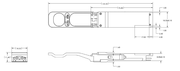
Dimension (Unit:mm)
PRODUCT CHARACTERISTICS
|
Parameter |
Value |
Unit |
Notes |
|
Module form factor |
QSFP+ |
|
|
|
Maximum aggregate data rate |
41.2 |
Gb/s |
|
|
Maximum data rate per lane |
10.3 |
Gb/s |
Higher bit rates may be supported. Please contact Irixi. |
|
Electrical interface and pin-out |
38-pin edge connector |
|
Pin-out as defined by the QSFP+MSA |
|
Maximum power consumption |
3.5 |
Watts |
|
|
Management interface |
Serial, I2C-based, 400 kHz maximum frequency |
|
As defined by the QSFP+ MSA |
|
Data Rate Specifications |
Symbol |
Min. |
Typ. |
Max. |
Units |
Ref. |
|
Bit rate per lane |
BR |
|
|
10, 313 |
Mb/sec |
1 |
|
Bit error ratio |
BER |
|
|
10-12 |
|
2 |
|
Link distance on SMF-28 |
d |
|
|
10 |
Kilometers |
3 |
Notes:
1.Compliant with 40GBASE-LR4 and XLPPI per IEEE 802.3ba.
2.Tested with a PRBS 231 -1 test pattern.
3.Per 40GBASE-LR4, IEEE 802.3ba.
ABSOLUTE MAXIMUM RATINGS
|
Parameter |
Symbol |
Min. |
Typ. |
Max. |
Units |
Ref. |
|
Maximum supply voltage |
Vcc1, VccTx, VccRx |
-0.5 |
|
3.6 |
V |
|
|
Storage temperature |
Ts |
-40 |
|
85 |
°C |
|
|
Case operating temperature |
Top |
0 |
|
70 |
°C |
|
|
Relative humidity |
RH |
0 |
|
85 |
% |
1 |
|
Damage threshold, per lane |
DT |
3.4 |
|
|
dBm |
|
Note:
1. Non-condensing.
ELECTRICAL CHARACTERISTICS (Top = 0 to 70°C, Vcc = 3.1 to 3.47 Volts)
|
Parameter |
Symbol |
Min. |
Typ. |
Max. |
Units |
Ref. |
|||||||
|
Supply voltage |
Vccl, VccTx, VccRx |
3.1 |
|
3.47 |
V |
|
|||||||
|
Supply current |
Icc |
|
|
1.13 |
A |
|
|||||||
|
Link turn-on time |
|||||||||||||
|
Transmit turn-on time |
|
|
|
2000 |
ms |
2 |
|||||||
|
Transmitter (per Lane) |
|||||||||||||
|
Single ended input voltage tolerance |
VinT |
-0.3 |
|
4.0 |
V |
|
|||||||
|
Differential data input swing |
Vin,pp |
120 |
|
1200 |
mVpp |
3 |
|||||||
|
Differential input threshold |
|
|
50 |
|
mV |
|
|||||||
|
AC common mode input voltage tolerance (RMS) |
|
15 |
|
|
mV |
|
|||||||
|
Differential input return loss |
|
Per IEEE P802.3ba, Section 86A.4.1.1 |
dB |
4 |
|||||||||
|
J2 Jitter tolerance |
Jt2 |
0.17 |
|
|
UI |
|
|||||||
|
J9 Jitter tolerance |
Jt9 |
0.29 |
|
|
UI |
|
|||||||
|
Data dependent pulse width shrinkage |
DDPWS |
0.07 |
|
|
Ul |
|
|||||||
|
Eye mask coordinates {X1, X2, |
|
0.11, 0.31 95, 350 |
Ul mV |
5 |
|||||||||
|
Y1, Y2} |
|||||||||||||
|
Receiver (per Lane) |
|||||||||||||
|
Single-ended output voltage |
|
-0.3 |
|
4 |
V |
|
|||||||
|
Differential data output swing |
Vout,pp |
0 |
|
800 |
mVpp |
6 |
|||||||
|
AC common mode output voltage (RMS) |
|
|
|
7.5 |
mV |
|
|||||||
|
Termination mismatch at 1 MHx |
|
|
|
5 |
% |
|
|||||||
|
Differential output return loss |
|
Per IEEE P802.3ba,Section 86A.4.2.1 |
dB |
4 |
|||||||||
|
Common mode output return loss |
|
Per IEEE P802.3ba,Section 86A.4.2.2 |
dB |
4 |
|||||||||
|
Output transition time, 20% to 80% |
|
28 |
|
|
ps |
|
|||||||
|
J2 Jitter output |
Jo2 |
|
|
0.42 |
UI |
|
|||||||
|
J9 Jitter output |
Jo9 |
|
|
0.65 |
UI |
|
|||||||
|
Eye mask coordinates #1 {Xl, X2 |
|
0.29, 0.5 150, 425 |
UI mV |
5 |
|||||||||
|
Y1, Y2} |
|||||||||||||
|
Power supply ripple tolerance |
PSR |
50 |
|
|
mVpp |
|
|||||||
Notes:
1.Maximum total power value is specified across the full temperature and voltage range.
2.From power-on and end of any fault conditions.
3.After internal AC coupling. Self-biasing 1OOΩ differential input.
4.10 MHz to 11.1 GHz range.
5.Hit ratio = 5 x 10E-5.
6.AC coupled with lOOΩ differential output impedance.
OPTICAL CHARACTERISTICS (Top = 0 to 70°C, Vcc = 3.1 to 3.47 Volts)
|
Parameter |
Symbol |
Min. |
Typ. |
Max. |
Units |
Ref. |
|||
|
Transmitter |
|||||||||
|
Signaling speed per lane |
|
|
|
10.3125 |
GBd |
1 |
|||
|
Lane center wavelengths (range) |
|
1264.5 - 1277.5 1284.5 - 1297.5 1304.5 - 1317.5 1324.5 - 1337.5 |
nm |
|
|||||
|
Total average launch power |
POUT |
|
|
8.3 |
dBm |
|
|||
|
Transmit OMA per lane |
TXOMA |
-4.0 |
|
3.5 |
dBm |
|
|||
|
Average launch power per lane |
TXPx |
-7.0 |
|
2.3 |
dBm |
2 |
|||
|
Optical extinction ratio |
ER |
3.5 |
|
|
dB |
|
|||
|
Sidemode suppression ratio |
SSRmin |
30 |
|
|
dB |
|
|||
|
Average launch power of OFF transmitter, per lane |
|
|
|
-30 |
dBm |
|
|||
|
Relative intensity noise |
RIN |
|
|
-128 |
dB/Hz |
3 |
|||
|
Optical return loss tolerance |
|
|
|
20 |
dB |
|
|||
|
Transmitter reflectance |
|
|
|
-12 |
dB |
|
|||
|
Transmitter eye mask definition {X1, X2, X3, Y1, Y2, Y3} |
|
{0.25, 0.4, 0.45, 0.25, 0.28, 0.4} |
|
|
|||||
|
Receiver |
|||||||||
|
Signaling speed per lane |
|
|
|
10.3125 |
GBd |
4 |
|||
|
Lane center wavelengths (range) |
|
1264.5 - 1277.5 1284.5- 1297.5 1304.5-1317.5 1324.5- 1337.5 |
nm |
|
|||||
|
Receive power (OMA) per lane |
RxOMA |
|
|
3.5 |
dBm |
|
|||
|
Average receive power per lane |
RXPx |
-13.7 |
|
2.3 |
dBm |
5 |
|||
|
Receiver sensitivity (OMA) per lane |
Rxsens |
|
|
-11.5 |
dBm |
|
|||
|
Stressed receiver sensitivity (OMA) per lane |
SRS |
|
|
-9.6 |
dBm |
|
|||
|
Damage threshold per lane |
PMAX |
|
|
3.3 |
dBm |
|
|||
|
Return loss |
RL |
|
|
-26 |
dB |
|
|||
|
Vertical eye closure penalty, per lane |
|
|
|
1.9 |
dB |
|
|||
|
Receive electrical 3 dB upper cutoff frequency, per lane |
|
|
|
12.3 |
GHz |
|
|||
|
LOS de-assert |
LOSD |
|
|
-15 |
dBm |
|
|||
|
LOS assert |
LOSA |
-28 |
|
|
dBm |
|
|||
|
LOS hysteresis |
|
|
1 |
|
dB |
|
|||
Notes:
1.Transmitter consists of 4 lasers operating at 10.3Gb/s each.
2.Minimum value is informative.
3.RIN is scaled by 10*log(10/4) to maintain SNR outside of transmitter.
4.Receiver consists of 4 photodetectors operating at I 0.3Gb/s each.
5.Minimum value is informative, equals min TxOMA with infinite ER and max. channel insertion loss.
