
单击打开
100G 光模块 CFP4 LR4
100G CFP4 LR4 optical Transceiver integrates receiver and transmitter path on one module. In the transmit side, four lanes of serial data streams are recovered, retimed, and passed to four laser drivers. The laser drivers control four EMLs (Electric-absorption Modulated Lasers) with center wavelength of 1296 nm, 1300nm, 1305nm and 1309 nm. The optical signals are multiplexed to a single –mode fiber through an industry standard LC connector. In the receive side, the four lanes of optical data streams are optically de-multiplexed by the integrated optical de-multiplexer. Each data stream is recovered by a PIN photo-detector and trans-impedance amplifier, retimed. This module features a hot-pluggable electrical interface, low power consumption and MDIO management interface.
The module provides an aggregated signaling rate from 103.125 Gbps to 111.81 Gbps. It is compliant with IEEE 802.3 ba 100GBASE-LR4 and ITU-T G.959.1, and OIF CEI-28G-VSR. The MDIO management interface complies with IEEE 802.3 Clause 45 standard. The transceiver complies with CFP MSA CFP4 Hardware Specification, CFP MSA Management Interface Specification, and OIF CEI-28G-VSR standards. A block diagram is shown in Figure 1.
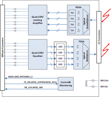
Figure 1. CFP4 LR4 Optical Transceiver functional block diagram
Transmitter
The transmitter path converts four lanes of serial NRZ electrical data from line rate of 25.78 Gbps to 27.95 Gbps to a standard compliant optical signal. Each signal path accepts a 100 Ω differential 100 mV peak-to-peak to 900 mV peak-to-peak 25 Gbps electrical signal on TDxn and TDxp pins. Inside the module, each differential pair of electric signals is input to a CDR (clock-data recovery) chip. The recovered and retimed signals are then passed to a laser driver which transforms the small swing voltage to an output modulation that drives a EML laser. The laser drivers control four EMLs with center wavelengths of 1295.56 nm, 1300.05 nm, 1304.58 nm and 1309.14 nm. The optical signals from the four lasers are multiplexed together optically. The combined optical signals are coupled to single-mode optical fiber through an industry standard LC optical connector.
Receiver
The receiver takes incoming combined four lanes optical data from line rate of 25.78 Gbps to 27.95 Gbps through an industry standard LC optical connector. The four incoming wavelengths are separated by an optical de-multiplexer into four separated channels. Each output is coupled to a PIN photo-detector. The electrical currents from each PIN photo-detector are converted to a voltage with a high-gain trans-impedance amplifier. The electrical output is recovered and retimed by the CDR chip. The four lanes of reshaped electrical signals are output to RDxp and RDxn pins.
PRODUCT FEATURES
Compliant with 100GBASE-LR4
Support line rates from 103.125 Gbps to 111.81 Gbps
Integrated LAN WDM TOSA / ROSA for up to 10 km reach over SMF
Digital Diagnostics Monitoring Interface
Duplex LC optical receptacle
No external reference clock
Single 3.3 V power supply
Case operating temperature range:0°C to 70°C
Power dissipation < 6W
Application
Local Area Network (LAN)
Data Center
Ethernet switches and router applications
STANDARD
Compliant to IEEE 802.3ba
Compliant to CFP MSA CFP4 Hardware Specification
Compliant to CFP MSA Management Interface Specification
Absolute Maximum Ratings
|
Parameter |
Symbol |
Min. |
Typ. |
Max. |
Unit |
Note |
|
Storage Temperature |
Ts |
-40 |
- |
85 |
ºC |
|
|
Relative Humidity |
RH |
5 |
- |
95 |
% |
|
|
Power Supply Voltage |
VCC |
-0.3 |
- |
4 |
V |
|
|
Signal Input Voltage |
|
Vcc-0.3 |
- |
Vcc+0.3 |
V |
|
|
Receive Input Optical Power (Damage threshold) |
Pdmg |
|
|
5.0 |
dBm |
|
Low Speed Electrical Characteristics
|
Parameter |
Symbol |
Min |
Typ. |
Max |
Unit |
Notes |
|||||||||||
|
Supply currents and voltages |
|||||||||||||||||
|
Voltage |
Vcc |
3.2 |
3.3 |
3.4 |
V |
With Respect to GND |
|||||||||||
|
Supply current |
Icc |
|
|
1.8 |
A |
|
|||||||||||
|
Power dissipation |
Pwr |
|
|
6.0 |
W |
|
|||||||||||
|
Power dissipation (low power mode) |
Plp |
|
|
1.0 |
W |
|
|||||||||||
|
Low speed control and sense signals, 3.3 V LVCMOS |
|||||||||||||||||
|
Outputs low voltage |
VOL |
-0.3 |
|
0.2 |
V |
IOH=100 μA |
|||||||||||
|
Output high voltage |
VOH |
Vcc-0.2 |
|
Vcc+0.3 |
V |
IOH=-100 μA |
|||||||||||
|
Input low voltage |
VIL |
-0.3 |
|
0.8 |
V |
|
|||||||||||
|
Input high voltage |
VIH |
2 |
|
Vcc3+ 0.3 |
V |
|
|||||||||||
|
Input leakage current |
IIN |
-10 |
|
10 |
μA |
|
|||||||||||
|
Low speed control and sense signals, 1.2 V LVCMOS |
|||||||||||||||||
|
Outputs low voltage |
VOL |
-0.3 |
|
0.2 |
V |
|
|||||||||||
|
Output high voltage |
VOH |
1.0 |
|
1.5 |
V |
|
|||||||||||
|
Output low current |
IOL |
4 |
|
|
mA |
|
|||||||||||
|
Output high current |
IOH |
|
|
-4 |
mA |
|
|||||||||||
|
Input low voltage |
VIL |
-0.3 |
|
0.36 |
V |
|
|||||||||||
|
Input high voltage |
VIH |
0.84 |
|
1.5 |
V |
|
|||||||||||
|
Input leakage current |
IIN |
-100 |
|
100 |
μA |
|
|||||||||||
|
Input capacitance |
C |
|
|
10 |
pF |
|
|||||||||||
|
MDC clock rate |
|
0.1 |
|
4 |
MHz |
|
|||||||||||
High Speed Electrical Specifications
|
Parameter |
Symbol |
Min |
Max |
Unit |
Notes |
|
|
Transmitter electrical input from host |
||||||
|
Differential voltage pk-pk |
|
|
900 |
mV |
|
|
|
Common mode noise (rms) |
|
|
17.5 |
mV |
|
|
|
Differential termination mismatch |
|
|
10 |
% |
|
|
|
Transition time |
|
10 |
|
ps |
20/80% |
|
|
Common mode voltage |
|
-0.3 |
2.8 |
V |
|
|
|
Receiver electrical output to host |
||||||
|
Differential voltage pk-pk |
|
|
900 |
mV |
|
|
|
Common mode noise (rms) |
|
|
17.5 |
mV |
|
|
|
Differential termination mismatch |
|
|
10 |
% |
|
|
|
Transition time |
|
9.5 |
|
ps |
20/80% |
|
Optical Transmitter Characteristics
|
Parameter |
Symbol |
Min |
Typ. |
Max |
Unit |
Notes |
|
Signaling rate, each lane |
|
|
25.78125 |
|
Gbps |
|
|
Lane wavelength(range) |
|
1294.53 |
1295.56 |
1296.59 |
nm |
|
|
|
1299.02 |
1300.05 |
1301.09 |
nm |
|
|
|
|
1303.54 |
1304.58 |
1305.63 |
nm |
|
|
|
|
1308.09 |
1309.14 |
1310.19 |
nm |
|
|
|
Rate tolerance |
|
-100 |
|
100 |
ppm |
From normal rate |
|
Side-mode suppression ratio |
SMSR |
30 |
|
|
dB |
|
|
Total launch power |
|
|
|
10.5 |
dBm
|
|
|
Average launch power, each lane |
Pavg |
-4.3 |
|
4.5 |
dBm
|
|
|
Extinction Ratio |
ER |
4 |
|
|
dB
|
|
|
Optical modulation amplitude, each lane (OMA) |
OMA |
-1.3 |
|
4.5 |
dBm |
|
|
Difference in launch power between any two lanes (OMA) |
|
|
|
5 |
dB |
|
|
Transmitter and Dispersion Penalty, each lane |
TDP |
|
|
2.2 |
dB |
|
|
Average launch power of OFF transmitter, each lane |
|
|
|
-30 |
dBm |
|
|
Relative Intensity Noise |
RIN20O MA |
|
|
-130 |
dB/Hz |
|
|
Transmitter reflectance |
|
|
|
-12 |
dB |
|
|
Transmitter eye mask {X1, X2, X3, Y1, Y2, Y3} |
|
{0.25, 0.4, 0.45, 0.25, 0.28, 0.4} |
|
|
||
Optical Receiver Characteristics
|
Parameter |
Symbol |
Min |
Typ. |
Max |
Unit |
Notes |
|
Signaling rate, each lane |
|
|
25.78125 |
|
Gbps |
|
|
Rate tolerance |
|
-100 |
|
100 |
ppm |
From normal rate |
|
Average receive power, each lane |
Pavg |
-10.6 |
|
4.5 |
dBm |
|
|
Receive max power, each lane (OMA) |
|
|
|
4.5 |
dBm |
|
|
Difference in launch power between any two lanes (OMA) |
|
|
|
5.5 |
dB |
|
|
Receiver Sensitivity (OMA), each lane |
Rsen |
|
|
-8.6 |
dBm |
1 |
|
Stressed Receiver Sensitivity (OMA), each lane |
SRS |
|
|
-6.8 |
dBm |
|
|
Stressed receiver sensitivity test conditions |
||||||
|
Vertical eye closure penalty, each lane |
VECP |
|
1.8 |
|
dB |
|
|
Stressed sys J2 jitter, each lane |
J2 |
|
0.3 |
|
UI |
2 |
|
Stressed sys J9 jitter, each lane |
J9 |
|
0.47 |
|
UI |
2 |
|
Receiver reflectance |
|
|
|
-26 |
dB |
|
|
LOS Assert |
LOSA |
-30 |
|
|
dBm |
|
|
LOS De-assert |
LOSD |
|
|
-12 |
dBm |
|
|
LOS Hysteresis |
|
0.5 |
|
4 |
dB |
|
|
1. Receiver sensitivity (OMA), each lane, is informative. 2. Vertical eye closure penalty, stressed eye J2 Jitter, and stressed eye J9 Jitter are test conditions for measuring stressed receiver sensitivity. They are not characteristics of the receiver. |
||||||
