
单击打开
25G SFP28 CWDM 10km
Features
Up to 25.78Gb/s data links
CWDM DFB laser and PIN receiver
Up to 10km on 9/125um SMF
Hot-pluggable SFP footprint
Digital diagnostic capabilities
Class 1 laser safety certified
Cost effective SFP28 solution, enables higher port densities and greater bandwidth
RoHS compliant and lead-free
Single +3.3V power supply
2-wire interface for management specifications compliant with SFF-8472 digital diagnostic monitoring interface for optical transceivers
All-metal housing for superior EMI performance
Case operating temperature
Commercial: 0 ~ +70℃
Extended: -10 ~ +80℃
Industrial: -40 ~ +85℃
Applications
High-speed storage area networks
Computer cluster cross-connect
Custom high-speed data pipes
Inter Rack Connection
HC’HCSC-FLxx11x 25Gb/s SFP28 transceiver consists of five sections: the LD driver, the limiting amplifier, the digital diagnostic monitor, the CWDM DFB laser and the PIN photo-detector .The module data link up to 10km in 9/125um single mode fiber.
The module optical connection is duplex LC and shall be compatible with SFP+ 28Gbps and backward compatible with legacy 10G SFP+ pluggable. The SFP28 CWDM LR module is a dual directional device with a transmitter and receiver plus a control management interface (2-wire interface) in the same physical package. 2-wire interface is used for serial ID, digital diagnostics and module control function.
The transmitter converts 25Gbit/s serial PECL or CML electrical data into serial optical data compliant with the 25GBASE-LR standard. An open collector compatible Transmit Disable (Tx_Dis) is provided. Logic “1” or no connection on this pin will disable the laser from transmitting. Logic “0” on this pin provides normal operation. The transmitter has an internal automatic power control loop (APC) to ensure constant optical power output across supply voltage and temperature variations. An open collector compatible Transmit Fault (Tx_Fault) is provided. TX_Fault is module output contact that when high, indicates that the module transmitter has detected a fault condition related to laser operation or safety. The TX_Fault output contact is an open drain/collector and shall be pulled up to the Vcc_Host in the host with a resistor in the range 4.7-10 kΩ. TX_Disable is a module input contact. When TX_Disable is asserted high or left open, the SFP28 module transmitter output shall be turned off. This contact shall be pulled up to VccT with a 4.7 kΩ to 10 kΩ resistor
The receiver converts 25Gbit/s serial optical data into serial PECL/CML electrical data. An open collector compatible Loss of Signal is provided. Rx_LOS when high indicates an optical signal level below that specified in the relevant standard. The Rx_LOS contact is an open drain/collector output and shall be pulled up to Vcc_Host in the host with a resistor in the range 4.7-10 kΩ, or with an active termination. Power supply filtering is recommended for both the transmitter and receiver. The Rx_LOS signal is intended as a preliminary indication to the system in which the SFP28 is installed that the received signal strength is below the specified range. Such an indication typically points to non-installed cables, broken cables, or a disabled, failing or a powered off transmitter at the far end of the cable.
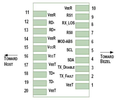
Pin Assignment and Pin Description
|
PIN |
Name |
Name/Description |
Notes |
|
1 |
VeeT |
Transmitter Ground |
1 |
|
2 |
TX_Fault |
Transmitter Fault |
|
|
3 |
TX_Disable |
Transmitter Disable; Turns off transmitter laser output |
|
|
4 |
SDA |
Two wire serial interface Data Line (LVCMOS-I/O) (MOD-DEF2) |
2 |
|
5 |
SCL |
Two wire serial interface Clock Line (LVCMOS-I/O) (MOD-DEF1) |
2 |
|
6 |
MOD_ABS |
Module Definition, Grounded in the module |
|
|
7 |
RS0 |
Rx Rate Select: |
|
|
8 |
RX_LOS |
Receiver Loss of Signal Indication Active LOW |
|
|
9 |
RS1 |
Transmitter Rate Select (not used) |
|
|
10 |
VeeR |
Receiver Ground |
1 |
|
11 |
VeeR |
Receiver Ground |
1 |
|
12 |
RD- |
Receiver Inverted Data Output |
|
|
13 |
RD+ |
Receiver Data Output |
|
|
14 |
VeeR |
Receiver Ground |
1 |
|
15 |
VccR |
Receiver Power - +3.3V |
|
|
16 |
VccT |
Transmitter Power - +3.3 V |
|
|
17 |
VeeT |
Transmitter Ground |
1 |
|
18 |
TD+ |
Transmitter Non-Inverted Data Input |
|
|
19 |
TD- |
Transmitter Inverted Data Input |
|
|
20 |
VeeT |
Transmitter Ground |
1 |
Notes:
1. Module ground pins GND are isolated from the module case.
2. Shall be pulled up with 4.7K-10Kohms to a voltage between 3.15V and 3.47V on the host board.
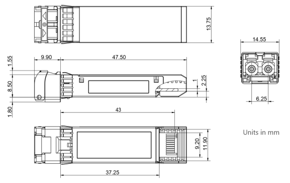
Mechanical Dimensions
Absolute Maximum Ratings
It has to be noted that the operation in excess of any individual absolute maximum ratings might cause permanent damage to this module.
|
Parameter |
Symbol |
Min |
Max |
Unit |
Notes |
|
Storage Temperature |
TS |
-40 |
85 |
oC |
|
|
Power Supply Voltage |
VCC |
-0.5 |
3.6 |
V |
|
|
Relative Humidity (non-condensation) |
RH |
5 |
95 |
% |
|
|
Damage Threshold |
THd |
3 |
|
dBm |
|
Recommended Operating Conditions and Power Supply Requirements
|
Parameter |
Symbol |
Min |
Typical |
Max |
Unit |
Notes |
|
TOP |
0 |
|
70 |
oC |
commercial |
|
|
-40 |
|
85 |
oC |
Industrial |
||
|
Power Supply Voltage |
VCC |
3.135 |
3.3 |
3.465 |
V |
|
|
Data Rate |
|
|
25.78 |
|
Gb/s |
|
|
Control Input Voltage High |
|
2 |
|
Vcc |
V |
|
|
Control Input Voltage Low |
|
0 |
|
0.8 |
V |
|
|
Link Distance (SMF) |
D |
|
|
10 |
km |
9/125um |
Electrical Characteristics
The following electrical characteristics are defined over the Recommended Operating Environment unless otherwise specified.
|
Parameter |
Symbol |
Min. |
Typ. |
Max |
Unit |
Notes |
|
Power Consumption |
p |
|
|
1.5 |
W |
|
|
Supply Current |
Icc |
|
|
450 |
mA |
|
|
|
||||||
|
Single-ended Input Voltage Tolerance |
Vcc |
-0.3 |
|
4.0 |
V |
|
|
Common mode voltage tolerance |
|
15 |
|
|
mV |
|
|
Differential Input Voltage Swing |
Vin,pp |
180 |
|
700 |
mVpp |
|
|
Differential Input Impedance |
Zin |
90 |
100 |
110 |
Ohm |
1 |
|
Transmit Disable Assert Time |
|
|
|
10 |
us |
|
|
Transmit Disable Voltage |
Vdis |
Vcc-1.3 |
|
Vcc |
V |
|
|
Transmit Enable Voltage |
Ven |
Vee |
|
Vee +0.8 |
V |
2 |
|
Receiver |
||||||
|
Single-ended Input Voltage Tolerance |
Vcc |
-0.3 |
|
4.0 |
V |
|
|
Differential Output Voltage Swing |
Vout,pp |
300 |
|
900 |
mVpp |
|
|
Differential Output Impedance |
Zout |
90 |
100 |
110 |
Ohm |
3 |
|
Data output rise/fall time |
Tr/Tf |
9.5 |
|
|
ps |
4 |
|
LOS Assert Voltage |
VlosH |
Vcc-1.3 |
|
Vcc |
V |
5 |
|
LOS De-assert Voltage |
VlosL |
Vee |
|
Vee +0.8 |
V |
5 |
Notes:
1. Connected directly to TX data input pins. AC coupled thereafter.
2. Or open circuit.
3. Input 100 ohms differential termination.
4. These are unfiltered 20-80% values.
5. Loss of Signal is LVTTL. Logic 0 indicates normal operation; logic 1 indicates no signal detected.
Optical Characteristics
|
Parameter |
Symbol |
Min. |
Typical |
Max |
Unit |
Notes |
|
Transmitter |
||||||
|
Center Wavelength |
λC |
λ -6.5 |
|
λ +6.5 |
nm |
|
|
Optical Spectral Width |
∆λ |
|
|
1 |
nm |
|
|
Average Optical Power |
PAVG |
-7 |
|
2 |
dBm |
1 |
|
Side Mode Suppression Ratio |
SMSR |
30 |
|
|
dB |
|
|
Optical Extinction Ratio |
ER |
3.5 |
|
|
dB |
|
|
Transmitter OFF Output Power |
Poff |
|
|
-30 |
dBm |
|
|
Transmitter and Dispersion Penalty |
TDP |
|
|
2.7 |
dB |
|
|
Optical Return Loss Tolerance |
ORLT |
|
|
20 |
dB |
|
|
Transmitter Eye Mask |
Compliant with IEEE802.3ae |
|
||||
|
Receiver |
||||||
|
Center Wavelength |
λC |
1270 |
|
1610 |
nm |
|
|
Receiver Sensitivity (OMA) |
Sen. |
|
|
-12 |
dBm |
2 |
|
Stressed Receiver Sensitivity (OMA) |
|
|
|
-9.5 |
dBm |
2 |
|
Average Receive Power |
|
-14 |
|
2 |
dBm |
|
|
Input Saturation Power (overload) |
Psat |
0.5 |
|
|
dBm |
|
|
LOS Assert |
LOSA |
-30 |
|
|
dBm |
|
|
LOS De-assert |
LOSD |
|
|
-15 |
dBm |
|
|
Damage Threshold |
THd |
3 |
|
|
dBm |
|
|
LOS Hysteresis |
LOSH |
0.5 |
|
|
dB |
|
The following optical characteristics are defined over the Recommended Operating Environment unless otherwise specified.
Notes:
1. Class 1 Laser Safety per FDA/CDRH and IEC-825-1 regulations.
2. Measured with Light source 1310nm, ER=3.5dB; BER =<10^-12 @ PRBS=2^31-1 NRZ.
Digital Diagnostic Functions
The following digital diagnostic characteristics are defined over the Recommended Operating Environment unless otherwise specified. It is compliant to SFF-8472 Rev10.2 with internal calibration mode. For external calibration mode please contact our sales staff.
|
Parameter |
Symbol |
Min. |
Max |
Unit |
Notes |
|
Temperature monitor absolute error |
DMI_ Temp |
-3 |
3 |
degC |
Over operating temp |
|
Supply voltage monitor absolute error |
DMI _VCC |
-0.15 |
0.15 |
V |
Full operating range |
|
RX power monitor absolute error |
DMI_RX |
-3 |
3 |
dB |
|
|
Bias current monitor |
DMI_ bias |
-10% |
10% |
mA |
|
|
TX power monitor absolute error |
DMI_TX |
-3 |
3 |
dB |
|
